Introduction:
PCBs, also known as Printed Circuit Boards, are the backbone of all electronics. You’ll find them in the tiniest of devices such as wearables to larger aircraft carriers. PCBs help mechanically support and electrically connect electronic components using conductive pathways called traces.
What is PCBA?
Contents
1 What is PCBA?
2 Prior to PCB Assembly:
3 Actual PCB Assembly Process Following are the steps in the general PCB assembly process:
4 Inspection/ Quality Control
5 Wave Soldering
6 First Article Inspection (FAI):
7 What is a First Article Inspection?
PCBA is the Printed Circuit Board Assembly i.e. the process of connecting electronic components to a PCB. Here we will break down the PCB assembly process step by step and all the basic parts of a printed circuit board.
Prior to PCB Assembly:
PCB Design Creation
Prior to PCB assembly, the PCB design is conceptualized. With the help of PCB layout software, the PCB design is created. It combines component placement and routing to create a blueprint for the contacts and layering of the PCB. This usually involves taking into account the size, dimensions, orientation, and type of PCB. There are a number of PCB design software programs you can choose from including EAGLE, Altium, EasyEDA etc.
DFM/DFA Check
Prior to assembly PCB design must be approved and checked for quality. This is done through the DFM(Design for Manufacturing)/DFA(Design for Assembly) check. Here the PCB is inspected to root out any defects or errors or potential manufacturing issues before the design is sent for fabrication. This is to avoid delays in product delivery. Any errors in design will render the PCB unusable.
PCB Fabrication
PCB fabrication is the process of the assembly of circuit boards from the PCB design. The PCB is composed of a number of components and the raw material is used to make up the actual board. A printed circuit board will usually include the dielectric, copper, silkscreen and solder mask.
Dielectric: Dielectric or dielectric material is a non-conducting material that forms the base of the printed circuit board. It is made of fiberglass which acts as an insulator and gives the PCB material strength.
Copper: Copper is used for both the coating of the PCB and as a copper foil which acts as a conductor and will form the circuit pattern after etching. Copper is what connects the various components together. The lines you see across a printed circuit board are actually copper traces.
Silkscreen: Silkscreen is a layer of ink used in PCBs to identify components, logos, symbols, and important information of the PCB.
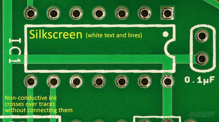
Image Courtesy: PCBgogo
Solder mask: Solder mask or solder resist is the top layer of the PCB which is applied to the copper traces of the printed circuit board to protect against oxidation caused by moisture and to prevent the formation of solder bridges.
Actual PCB Assembly Process
Following are the steps in the general PCB assembly process:
Application of Solder Paste
In the first step, once the board is ready, the solder paste is applied to the board. Actually, the solder paste is applied to only certain areas of the PCB where the components will be added. It helps bind the components to the PCB. In the use of SMT (Surface Mount Technology) for PCB, the solder paste is applied by solder printing. By taking a stencil with cutouts and using it to apply solder paste so it is only applied to the contacts.
Usually, after the solder paste application, inspection follows so errors are identified, either manually or via machine.
Pick and Place
Once the solder paste is applied, the next step involves a pick and place machine, which will pick up surface mount components and place them on the PCB contacts which are then soldered in the next step. The machine will pick up the components with a vacuum grip and carefully place them at the required positions.
Reflow Soldering
In the next step, the solder needs to solidify. This is done through a reflow method. The PCB is shifted to a conveyor belt which carries the PCB to a reflow oven heated to around 250 degrees Celsius. Here the solder melts while the PCB moves on to a set of coolers which allows the solder to solidify gradually by cooling down. In this way, the components are permanently soldered to the PCB. Special attention needs to be given to the amount of heat supplied so as not to damage the components.
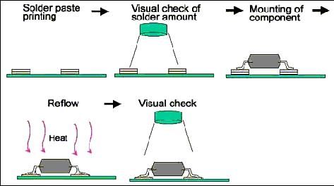
Image Courtesy: wonderfulpcb.com
Inspection/ Quality Control
In the next step, the PCB is sent for X-ray inspection. This is used to test the quality of the solder joints. X-ray inspection is generally used for more complex PCBs. The X-ray will allow you to visualize the lower layers of the PCB to identify any hidden errors in assembly. The X-ray will show the accuracy of the soldering and defects (if any). Defects may include open solder joints i.e. Incomplete soldering, component misalignment etc.
As mentioned before X-ray inspection is generally used for more complex PCBs so it is a rarer type of inspection. Other common types include manual checks and automated optical inspection.
Wave Soldering
If you’d prefer not to use the reflow soldering process, you can go for the wave soldering process which is a sort of automated version of manual soldering. However, this type of soldering is typically used for plated through-hole (PTH) components.

Here, the PCBs are placed on a conveyor belt which runs over a wave of molten solder on its underside. In this way, the contact points of all the components will be soldered on the underside.
First, a flux spray is used to prevent oxidation of the PCB. Then the PCB is preheated. Then the wave of molten solder is applied and finally, the solder cools down and solidifies.
Testing
After soldering is completed, the PCB must be tested. This the quality assurance testing to identify any potential errors or flaws from manufacturing.
First Article Inspection (FAI):
This is also a rarer type of inspection, a lot less common than the X-ray inspection, visual inspection types. You need to check with your manufacturer while drawing the PCB design for fabrication to see whether or not it can conduct first article inspection.
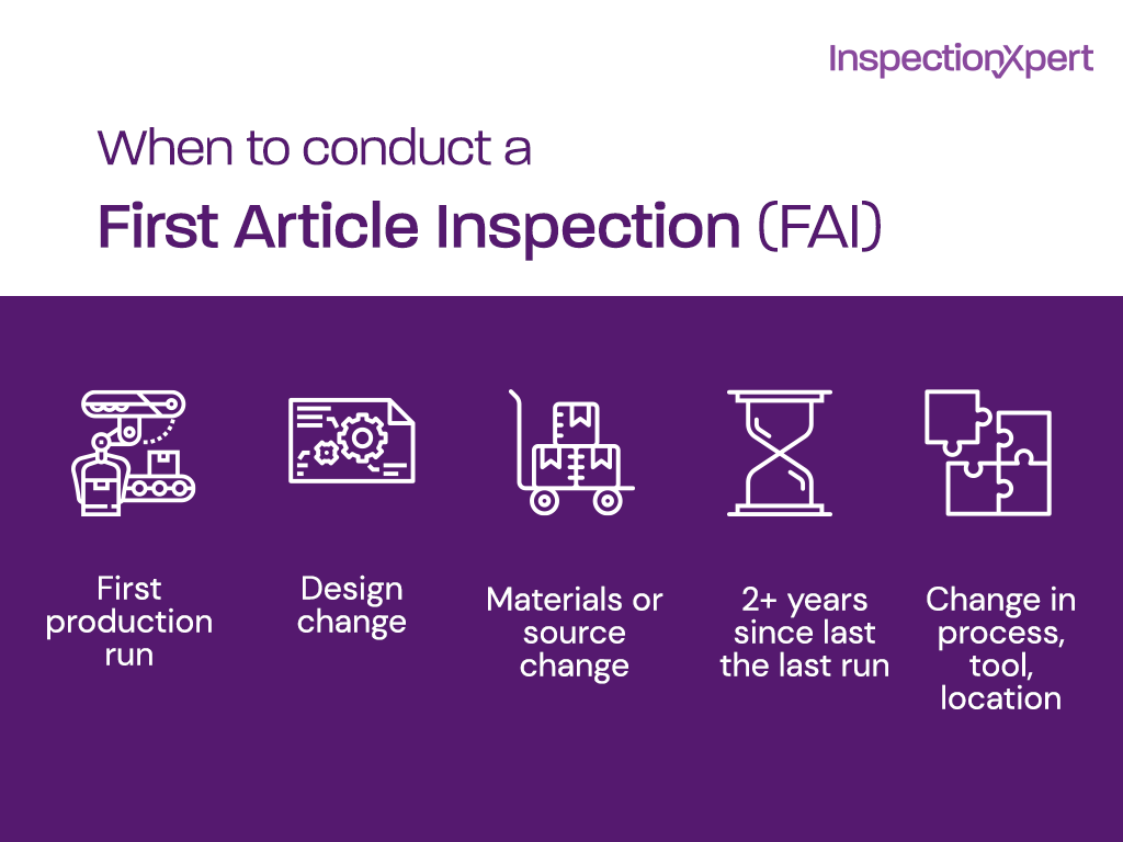
image Courtesy: InspectionXpert
What is a First Article Inspection?
The first articles are the first PCBs produced from the first mass production line, it can be a random sample from the first production run. Testing at this stage will see whether or not the product fits your requirements and if the manufacturing process is accurate enough.
First Article Inspection can be done by the customer who would either visit the facility or have the product delivered to them. It can also be done online through photographic samples and testing results shown to the customer. Or, it can be done by the manufacturer at the facility. However, there is always a chance that the manufacturer might miss any details you might be looking out for. This is why inspection done with the customer would be more recommended.
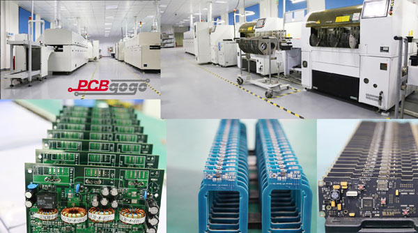
The main goal is to find out whether the PCB assembly process can mass manufacture high-quality yields. Any defects found are resolved so the assembly process may continue. A question may arise here; if you already have pre-production samples or prototypes then is there any need for first article inspection? The answer, yes. PCB assembly prototypes are not exactly first articles as they are manufactured through a different process and are not taken from mass production lines, as compared to the first articles that are taken from the assembly production line.
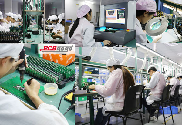
PCBgogo, one of the largest and most popular PCB manufacturers in Shenzhen, China. Built over 2400 sqm of land, this company specializes in manufacturing high-quality PCB’s (Printed Circuit Boards) at a low price.
These boards are custom designed according to your needs. Just looking at the “product categories” PCBgogo specializes in, we realize how much they have expanded over the years. These categories include data communication, optical networking, medical treatment, industrial control, aerospace/military, etc. just to name a few.
This article is originally published on electronicslovers.com and authorized to reprint on pcbgogo.
The original link: https://www.electronicslovers.com/2020/11/pcb-assembly-process-and-first-article-inspection.html
- Comments(0)
