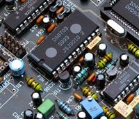
In the manufacturing process of PCBs, electrical defects such as short circuits, open circuits, and leakage might occur due to external factors. As PCBs continue to evolve towards high density, fine pitch, and multi-layers, the difficulties and cost of rework will significantly increase if the defective board is not screened out at an early stage and flow into the following-up process. To improve the rate of qualified products, electrical testing must be conducted in the PCB manufacturing process.
Some key terms:
Net: A net on a printed circuit board is a set of points that are electrically connected to a start and endpoint by the traces we design. It includes component pads, traces, test points (if any), and copper planes associated with the same connection.
Netlist: It refers to a connected group of two or more points in a PCB that share common electrical properties.
Main procedures of electrical testing
Capacitance Testing:
It is to detect the shorts on the board. By applying a charge to reflect the capacitance in the different Nets, it compares its value with the value of the board under test and generates a Netlist where the measurement does not correspond.

Continuity Test
This test is designed to detect shorts between different Nets making up the circuit to ensure that no current flows between them.

Insulation testing
Some small cooper residues may remain on the board surface after the chemical manufacturing process of the PCBs. They would not necessarily lead to shorts but may shorten the width of the traces. This testing is to find out these defects between the Nets to avoid unexpected electrical interactions such as voltage jumps or current leakage.

Types of electrical testing
Bed of nails testing
The bed of nails tester is a relatively traditional testing method that requires specific fixtures that contain standoff pins and plexiglass layers with holes drilled to support the springs pins. Fixtures with springs are attached to each test point on each board. The spring can provide each test point with 100g-200g pressure to ensure good contact with the test point. Arranged in a matrix that looks like a bed of nails, these fixtures are controlled by testing software and programming. With these testers, we are able to verify the condition of all the test points.
This test method requires specific fixtures, and the storage of the fixtures also takes up space, which is not economical. But its test speed is fast, and the fixture can be used repeatedly, making it an ideal testing method for batch PCB production.
Flying probe testing
The flying probe test uses 4 to 8 probes to conduct high-voltage insulation and low-resistance continuity tests on the circuit board. During this process, the board is placed vertically in the frame. The test probes are moved in the XY direction on both sides of the circuit to be set exactly on the pads whose electrical characteristics need to be tested. The test leads are then moved on the Z-axis until they make contact with the pads. The whole testing process is computer-controlled and the software will perform the required measurements and display the results to determine if the board is correct (PASS) or rejected (FAIL).

Flying probe testing machine in PCBGOGO
Flying probe testing is the most widely used method today, offering greater reliability. Its testing speed is slower than the bed of nails tester, taking several minutes to complete the test on a single board. However, it doesn't need specialized fixtures that require several days to develop the testing device, which significantly reduces product design cycles and time-to-market. This quality makes it an effective option for PCB prototypes and small-batch production. As a professional PCB manufacturer, PCBgogo conducts flying probe testing on every board before being delivered to the customers.

Flying probe testing lines in PCBGOGO
Conclusion
Electrical testing is a necessary part of PCB manufacturing. It can find out the defects at an earlier stage, help save money and prevent issues before reaching the final production phase. However, electrical testing can only detect certain defects on PCBs.An appropriate combination of other testing techniques should be conducted during different production stages to ensure that customers get error-free boards.

