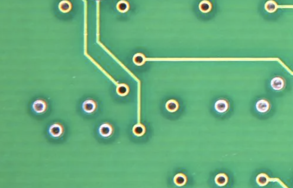
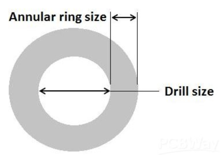
Annular rings are the donut-shaped copper areas on vias or holes when you look at the PCB from the top. It is the area between the drilled hole and the edge of the conductive cooper pad. The annular rings have different widths based on the purpose of the PCB design and space constraints. If there are problems with the annular rings, the trace continuity and the circuit functionality will be affected.

____________________________________________________________________________________________________________________________
Common issues with the annular rings
A perfect annular ring will be created by drilling right into the center of the via pad. However, the annular ring may not be in the center because the drilling accuracy depends on the drilling machine used by the PCB manufacturer. There are several drill issues with the annular ring:
l Good via
When the via is in the center of the pad or the given limit area, we call the via is a good via, which will result in a nice donut-shaped annular ring and good electrical connectivity.
l Tangency:
When the driller is not aligned with the mark, the finished hole will be off-center and near the side of the pad. An annular ring tangency will appear when a part of the hole contacts the edge of the pad.
l Breakout:
If the hole deviates a lot, a breakout occurs when a portion of the hole exceeds the padded area. This is a kind of undesired annular ring, which may cause short circuits and failure connectivity.
____________________________________________________________________________________________________________________________
The importance of the drilling accuracy
Then we can know that the drilling accuracy is critical to minimize the annular ring, especially for PCB drilling on smaller and dense PCBs. The existence of the annular ring allows the via not have to be precisely located in the middle of the ring and still can ensure a good electrical connection. Usually, as long as it is inside the pad and does not affect the electrical connection, it is also acceptable even the ring touches the pad’s boundary.
Sometimes, engineers may design very smaller annular rings when the space between nearby components. But this will increase the chance of vias very close to the edge of the ring, which may cause an annular ring breakout. Therefore, for a good result of the annular ring, PCB manufacturers should pay more attention to the produce accurate annular rings, and PCB designers are also better to leave more space to allow additional tolerance.
____________________________________________________________________________________________________________________________
Annular ring technology at PCBGOGO
The perfect width of an annular ring is the calculated like this:
Annular ring width = (pad diameter – drill diameter) / 2

Generally, according to the drilling capability of PCBGOGO, the minimum width of the annular ring is 0.15mm, and the drill size (CNC) ranges from 0.2mm to 6.3mm. Extra charges may be caused if the via size is out of the range.
Please remember that you would better to keep enough space when you design your PCB vias and know more about the manufacturing tolerance before you place orders. These can help to keep the width of the annular rings in an acceptable distance and ensure the electrical connection not to be affected. Please trust us, whether it is PCB prototype assembly or small batch production, experts from PCBGOGO will provide you with the most appropriate assistance for your PCB design.
