How does double-sided SMT assembly work?
Surface Mount Technology(SMT) is used in attaching electrical components to a printed circuit board, where the components are attached on the surface of the PCB without drilling holes. Double-sided SMT (Surface Mount Technology) assembly enables components to be mounted on both sides of a PCB, maximizing PCB functionality while minimizing size. Now, let us have a look at how the double-sided SMT assembly works and its key process steps.
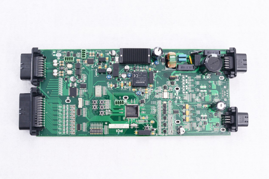
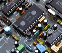
SMT assembly by PCBGOGO
What is Double-Sided SMT Assembly, and Why Use It?
SMT assembly stands for Surface Mount Technology assembly, and it is a type of soldering technology that employs reflow soldering or other defined processes to mount electronic components on a printed circuit board. This process is complex and has to be divided into single-sided and double-sided SMT.
Double-sided SMT is a process that makes use of double-sided PCBs ------ Side A and Side B are populated with surface-mount components. This means that both the bottom and the top layers have conductive paths, and designers can place more components on both sides. Increased layout space improves electrical performance and reduces PCB size, allowing for compact products with better portability and complexity.
This allows modern electronic designers to take full advantage of the entire usable board area, enabling higher density and more compact circuitry. The assembly process is somewhat complex since it also involves the use of complex components. Next are two methods to assemble double-sided PCBs.
Double-sided SMT Assembly Process (Method A: Two-Side Reflow Soldering)
This is the most widely used modern method for assembling double-sided PCBs. It is almost similar to the general SMT assembly process, but only a few steps will be added. Two sides of the PCB apply solder paste + component placement + reflow soldering, ensuring high precision and reliability. Here is the full process of Double-sided reflow assembly using solder paste.
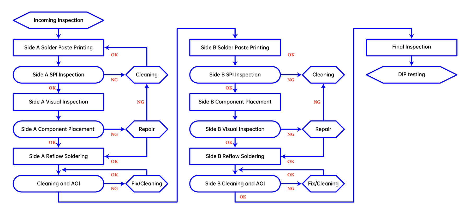
Step 1: Side A Solder Paste Printing
The first side(Side A) goes through stencil printing, and the solder paste is applied to the surface-mount pad accurately. Proper alignment, printing thickness, and stencil cleanliness are vital to avoid solder bridges and insufficient solder.
Step 2: Side A SPI Inspection
Solder Paste Inspection(SPI) is optional, but PCBGOGO processes it for each board. It is to check the volume, area, and height of the printed solder paste to ensure printing consistency.
Step 3: Side A Component Placement
Pick-and-place machine places components on the printed solder paste, and the paste temporarily fixes components in place.
Step 4: Side A Reflow Soldering
Reflow Side A in the reflow oven. The machine gradually heats the board, helping the solder paste melt and then cool the board down to solidify the solder joints.
Step 5: Side A Cleaning and AOI
After reflow, the assembly cools down naturally. Cleaning is also optional, but it is performed for no-clean or water-soluble solder pastes when necessary. AOI is done to inspect and repair possible problems.
→ Then, side A is finished. The board will be turned over with fixtures or conveyors to prevent pressure on the soldered components. Then, repeat the same steps as side A.
Step 6: Side B Solder Paste Printing
Step 7: Side B SPI Inspection
Step 8: Side B Component Placement
Step 9: Side B Reflow Soldering
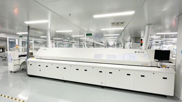
Reflow oven in PCBGOGO
Step 10: Side B Cleaning and AOI
Step 11: Final Inspection(X-ray/OQC)
Final inspection is done for ultimate quality assurance. X-ray inspection may be used for BGAs or QFNs.
In some double sided PCB assembly processes, another step ------ inserting and soldering through-hole components, is also necessary. These components go into holes and connect to two sides of the board to increase mechanical strength and ensure stable electrical connections.
Double sided SMT Assembly Process(Method B: Adhesive +Wave Soldering)
Compared with the general double-sided SMT process using solder paste + reflow, the adhesive + wave-soldering method is a more traditional assembly approach that has been widely used for decades in high-volume PCB manufacturing. The following steps are involved.
Wave Soldering Double Sided SMT Assembly Process
1. Incoming Inspection
The inspection of the assembly files is done to ensure they meet the standards of the designer. Files include Gerber, BOM, placement files, and more.
2. Screen solder paste printing on side A.
Side A is the first side to be printed. The process on side A is done similarly to what is done while doing the single-sided SMT assembly.
3. Surface Mounting
Pick-and-place machines mount components onto the solder-pasted pads.

Pick&Place machine in PCBGOGO
4. Drying
Remove moisture from both PCB and solder paste, preventing solder splatter or void formation during reflow.
5. Reflow soldering on Side A
The board, after component mounting on side A, is sent through the reflow oven. In this process, solder paste melts and form solid joints.
6. Clean out
Removes flux residues or contaminants to ensure reliable adhesion and downstream processing stability.
7. Plate turnover
The turnover is special to allow printing of side B of the double-sided PCB.
8. Adhesive Dispensing on Side B
Secure B-side components during wave soldering and prevent them from being washed off by the solder wave.
9. Surface mounting
10. Drying
11. Wave soldering the PCB side B
Here, SMT wave soldering is preferred as compared to reflow soldering because it will protect the printed side A from remelting.
12. Cleaning out
13. VI & AOI
This is where the visual inspection and automated optical inspection is done for quality to make sure that the design has no defects.

AOI in PCBGOGO
Brief Explanation of Wave Soldering SMT Assembly Process
1. Dispensing
Since the type of board that is generally used in this process is the double-sided printed circuit board, to prevent the components that were soldered on the input side of the board from undergoing melting and re-sold off because of remelting of the solder mask, it is advised that a dispenser is installed at the input surface. A water droplet at the input of the printed circuit board is employed to fix the electronic components to the board.
2. Component placement
The purpose of this process is to make sure that the surface mount components are accurately fixed at the exact required position on the printed circuit board. A Pick&Place machine is used to ensure that the process is achieved.
3. Curing
This one is used to aid in melting the patch glue, and this helps to ensure that the components and the printed circuit board are strongly bonded together.
4. Reflow soldering
This does the melting of the solder paste with the SMT reflow soldering furnace, so as to ensure that the SMT components and the printed circuit boards are bonded together.
5. Cleaning
This is the process where the harmful soldering residues, such as the flux, are removed from the SMT assembled printed circuit boards.
6. Inspection
Here, the welded board assembly quality is put to the test to ensure that whatever was done is correct and of great quality. The magnifying lens, online tester, microscope, AOI, flying probe tester, etc., are used to ensure that the process is done well.
7. Rework
Here, we involve PCBs that have a failure detected. The PCB is reworked to remove the failure.
Summary
Double-sided SMT assembly is a very necessary process when it comes to assembling PCBs with more than one layer. Mostly used when the top and bottom layers of the PCB are to be printed. The process and the machines used in the process have been highlighted.
PCBGOGO is a fabricating house that could solve your PCB fabrication challenges. As a leading double-sided PCB assembly manufacturer, we have 6 SMT production lines with professional engineering support and rigorous quality control, supporting full-service PCB assembly solutions------from prototypes to mass production. You can submit your Gerber files and BOM for an instant and transparent quote through our online system. Contact us now to get professional PCB solutions.


