PCB Trace - Everything You Need To Know
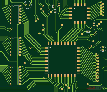
When it comes to printed circuit boards, trace is mainly in referring to the network of copper, wiring, insulation, as well as fuses that is made up of the board. In general, there will a great possibility that the PCB trace is inconsistent if it has some wrong with any given electronic device. What’s more, trace resistance is the most common term used by electronic engineers in the printed circuit board industry. As well as the trace resistance means the parts of a PCB that resist the flow of a current.
What is PCB trace?
PCB trace is important for each PCB like a current, and it will spend more time and energies on fitting if make it wrong to detect or calculate the trace. What’s worse, it may lead to making mistake in the system for any device.
There are many components in the printed circuit board and you should understand which parts and materials do you need as repairing or assembling the printed circuit board. as well as what kinds of functions and formulas you should take.

PCB trace thickness
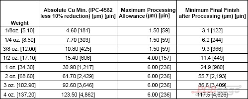
For electronic designer, the thickness of PCB plays an important role in the PCB design. The thickness can keep the balance, however, there will not function or lead to damage for the circuit board, as well as involving the components connected to the board. So the PCB thickness will change as the types of PCB change, because there are single-sided PCB, double-sided PCB, multilayer PCB in the electronic market. And there are some common PCB trace thickness ranging from 0.008 inches to 0.240 inches, such as 0.2 mm (0.0079 inch), 0.4 mm (0.016 inch), 0.5 mm (0.020 inch), 0.6 mm (0.024 inch), 0.8 mm (0.032 inch), 1.0 mm (0.04 inch), 1.2 mm (0.047 inch), 1.5 mm (0.062 inch), 1.6 mm (0.063 inch), 2.0 mm (0.079 inch), 2.3 mm (0.091 inch) and so on.

PCB trace width calculator
As you know, PCB trace width is an important design parameter in PCB design. And it’s necessary for you to have an adequate trace width so that make sure it can transfer the desired amount of current without overheating and damaging your board. You can calculate an estimate of the minimum trace width for a given current and copper weight with PCBGOGO online tool. And a higher current needs the thicker traces while a thicker copper weight allows for thinner traces.
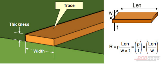
The below is the formula for resistance of a trace:
Resistance = Resistivity*Length/Area*(1 + (Temp_Co*(Temp - 25))
Where, Area = Thickness*Width
A copper Thickness of 1 oz/ft^2 = 0.0035 cm
Copper Resistivity = 1.7E-6 ohm-cm
Copper Temp_Co = 3.9E-3 ohm/ohm/C
Voltage Drop is Current * Resistance
Power Loss is Current^2 * Resistance

Something you need to know before calculating trace width
calculating trace width is much more complicated than any given conductor. There are a lot of things you need to know before calculating the PCB trace width. First of all, you need to know the maximum current that it can function for the board as inputs, which include the unit of the measurement trace, the trace thickness, temperature of the trace, as well as the ambient temperature of the trace. It will make an effect on the input ranges of the width.
You will get the output figures when you plug in the numbers into the calculator. And the figures of trace width include the trace width (measured in amps), resistance (measured in ohms), the trace temperature (measured in Celsius), the voltage drop (measured in volts), and the power dissipation (measured in watts), which make it clear to tell you what the trace width is.
PCB trace current
A direct current is used in PCB current source as a power source, which refers to that there is only one flow of a current passing through the wiring and copper of the board where the electronics pass straight to the battery, and then powers any given device. PCB trace current has a great different with a PCB trace, which offers how the wiring and other conductors interact with each other to provide the current.
It’s important for PCB trace current to recognize because they are as necessary as the trace resistance and trace width in the PCB fabrication. What’s more, there is no current in any given PCB, there is no power. Make it correct to measure the trace and trace width of any given PCB, however the components can’t function well and it will need to repair if there is only one error in the PCB trace current.

Conclusion
In fact, PCB trace has a great effect on fabricating the circuit board, there are a misunderstand, which have no idea about the PCB trace and PCB trace width are as important as calculating and determining the PCB current. So learn more information about PCB trace before design your PCB.
PCBGOGO can offer you instant quote, on one hand, we are highly specialized not only in quick-turn PCB prototype and PCB assembly, but also medium and small volume PCB fabrication. Such as 24 hours lead time, 24 hours components quote, as well as 24 hours prototype PCB assembly. And we will try our best to meet your demands on fabricating PCB and committed to adhering to the strictest standards in PCB fabrication and assembly.
Please feel free to contact us with service@pcbgogo.com if you have any questions, we will be happy to help you.
