An Introduction to The PCB Lamination Process by PCBGOGO
In the filed of electronics, it’s a great attribute for reliability of the electronic circuits. The users have high expectation for the perfect devices so that there is no interruption, as well as the device can operate for a long term. So it can’t be denied that it needs to have a robust and unfailing protection from intense and drastic condition for high quality operation.
Needless to say, lamination provided to the board is the basic protection to be provided to the printed circuit board. What’s more, a printed circuit board is essentially a board or a card which offers methods and means (electronic and physical of connecting the electronic components).

Introduction
A printed circuit board is a structure used to connect and support electronic components, which is made up of laminate including mostly glass epoxy base material with coating of copper on single or either side of it. And the boards have conductive pathways through which different components are connected across the board. These pathways are etched from copper sheets. To ensure that the copper layer does not conduct a signal or current, it is laminated into a substrate. However the lamination requirements of various kinds of printed circuit boards depend upon their nature, type and the area of use.
Multiple layer PCBs
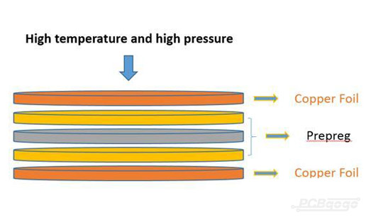
Circuit boards that are made up of various layers are known as multi-layer PCBs. The layers can be either thin etched boards or traces layers, in both cases, they are bonded with lamination. What’s more, for lamination, the internal layers of the boards are subjected to under pressure (275 to 400 psi) and extreme temperature (375o F). so it will be done as laminating with a photosensitive dry resist. The PCB is allowed to cure at a high temperature, the pressure is slowly released and then the material is slowly cooled.
Double-sided PCBs
It has a difference from other types of PCBs for the fabrication aspects of double-sided PCBs, but lamination process is very similar. As shown in the multilayer PCB, the PCB panel is laminated with a photosensitive dry resist under extreme temperature and pressure.
Sequential lamination
Printed circuit boards can be comprised of two or more subsets if you use the sequential lamination technology. The subsets, multi-layer PCBs created in separate processes, are pressed together and a dielectric element is interposed among each pair of subsets. It is subject to the standard manufacturing steps after this process.
Teflon (PTFE) microwave laminates
PTFE microwave laminates are one of the most used laminates for PCB lamination. And they are a type of laminate that has a very low electrical loss, consistent dielectric constant and tight thickness tolerance---all required for certain applications such as radio frequencies. One common way of laminating PTFE laminates is with CTFE (chlorotrifluoroethylene) thermoplastic film. A pressure of 100 to 200 psi is maintained through the entire lamination process. It is heated until it reaches 400 degrees Fahrenheit, where it is cured, then is slowly cooled.

Conclusion
With over 10 years as an industry leader, PCBGOGO is one of the most experienced PCB and PCB assembly manufacturer in China. highly specialized not only in quick-turn PCB prototype and PCB assembly, but also medium and small volume PCB fabrication. we specialize in the lamination and sequential lamination requirements of the circuits in order to ensure the long term cost effective working of the electronic devices. What’s more, we will try our best to fabricate your PCBs with the highest quality to meet your demands and committed to adhering to the strictest standards in PCB fabrication and assembly.
If you have any questions, please feel free to contact us with service@pcbgogo.com, we will be happy to help you.
