PCBGOGO Multiple Layers PCB Standard Stack-up
Many customer will question about the standard stackup of multi-layers PCB in our company. Here is the standard stackup of multiple Layers PCB in PCBGOGO.
4 layer PCB stack-up


6 layer PCB stack-up


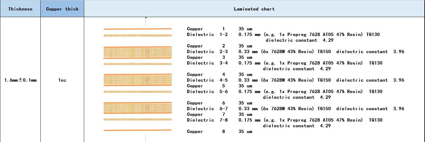
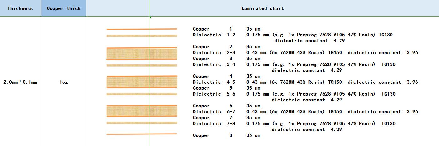
8 layer PCB stack-up


![]()
Notes:
1.
Above stackup lists are our factory’s standard stackup of 4-layer PCB.
2.
2. The outer and inner copper thickness of 0.8-2.0mm PCB are both 1oz, while 0.6mm PCB only has 0.5oz inner copper thickness.
3. 1.6mm and 2.0mm PCB can be made with 2OZ outer copper thickness and 1.5OZ inner copper thickness.
4. When copper thickness increases, the dielectric layer will be reduced correspondingly, and the final board thickness will have positive and negative tolerance ±0.1mm.
5. This layer pressure diagram is for reference only, we have the highest interpretation rights in the laminating process, if there is any question, please contact the manager!
