WHAT ARE GOLD FINGERS?
With the development of PCB industry, gold fingers play an important role in inner-workings of computer technology, and today there are a lot of industrial processes achieving with gold fingers. So what are gold fingers?
There are three various methods that come with printing the prototype PCB’s legend for design engineers in the fields of PCB fabrication and assembly. And the legend is what the design engineers use to figure out the component designators, switch settings and test points of PCB, which are very important for assembling, testing and servicing the circuit board prototype. However, there are more things that go into the legend, including gold fingers. PCBGOGO will make an introduction about the gold fingers.
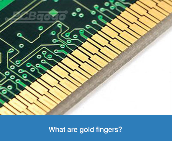
What Are Gold Fingers?

Gold fingers are the gold-plated connectors that run on the edges of the printed circuit board prototype, and they aim at connecting the secondary circuit board to the motherboard of a computer. Also, the gold finger is used for different devices that communicate with digital signals, for example, smartwatchs and smartphones. Because the alloy has a great conductivity, gold is used in the connecting points along the board.
At present, there are types of gold used in the process of PCB gold finger plating:
Electroless Nickel Immersion Gold (ENIG): it’s more cost-effective and make it easier to solder than electroplated gold, however, it’s softer, thin (in general, 2-5u” composition, which it’s not appropriate for the abrasive effects of PCB removal and insertion.
Electroplated Hard gold: the gold is hard and thick (typically 30u”), so it’s more better for the abrasive effects of constant PCB usage.
The plating process needs to do in steps that finishing the surrounding details on the board first for the combination of gold finger. When it needs to plate the fingers, the nickel is applied on the copper. And then apply the surface finish last. So check the board under a magnifying lens and do the adhesion test after everything is ready.
Each board needs to do a series of inspections and defect tests to make sure the fingers and slot are suitable for hand-in-glove. If the gold plating on a PCB is lack of smoothness or it does not adequately adhere to the surface, which will happen to some defects.
How Are Gold Fingers Applied?

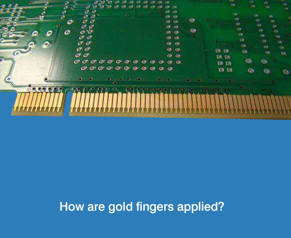
Gold fingers can be used for many various things. And they use depending on the designer’s purpose. There are some common applications of gold fingers as the follows:
1. Provide an interconnection point for transferring network data;
2. Connect external components to the PCB prototype;
3. A place for attaching specialized adapters or daughter boards;
4. Serve as an audio adapter;
Gold Finger Specifications You Should Know

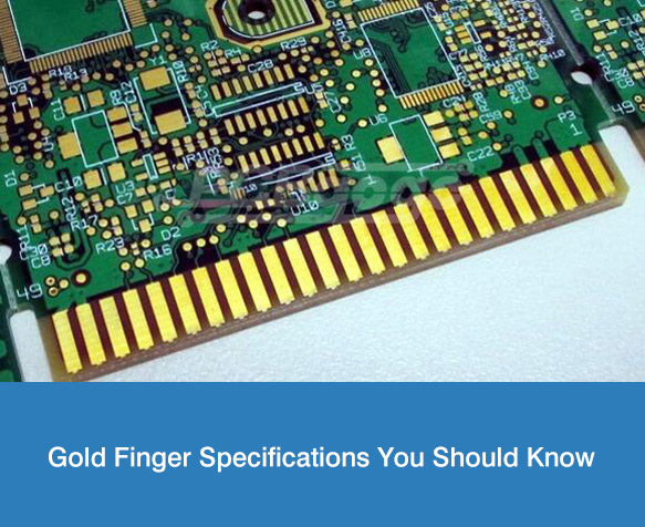
There are some standards you need to follow for the gold fingers so that it can work correctly during the plating process of gold finger. As well as the PCB design need to take into account the areas where is necessary to proper finger length and alignment. The rules can be used for the gold finger design as the follows no matter what the size or the purpose of the circuit board:
1. Plated through hole should far away from the gold fingers;
2. There should be kept at a distance between gold fingers and solder mask or screen printing;
3. Gold fingers should always keep the opposite direction from the middle of the board.
If you don’t follow these rules during the plating process of PCB gold finger, the circuit board may be unable to communicate with the parent board. Alternately, the board might not be unsuitable for the corresponding slot on the motherboard.
In 2002, the Association Connecting Electronics Industries (IPC) established the production standards of PCB gold fingers. With the release of IPC-4556, the standards were amended in 2012. In 2015, the standards were amended again as the release of IPCA-600 and IPC-6010, which are now the most widely used in PCB production. And the IPC standards can be categorized as follows:
Chemical composition: the gold plating should include the cobalt between 5 and 10 percent if you want there are the maximum rigidity along the edges of PCB contacts.
Thickness: the plating thickness of gold fingers should always keep within the range of 2 to 50 microinches. And the standard thickness of size are 0.031 inches, 0.062 inches, 0.093 inches and 0.125 inches. In general, the lower thickness is used for PCB prototype but the higher thickness is used along connecting edges that are regularly inserted, unplugged and reinserted.
Visual test: the gold fingers should do the visual test with a magnifying lens. The edges should have a clean and smooth surface, as well as there are not excess plating or nickel appearance.
Tape test: it recommends the IPC to do a test with placing a strip of tape along the contact edges for testing the adhesiveness of the gold plating along the contacts. To check the strip whether there is traces of plating after removing the tape. The plating will be lack of enough adhesiveness along the contacts if there is evident gold plating on the tape.
PCB Gold Finger Beveling

You can use the plating process of gold finger on the circuit board before the surface finish and after the solder mask. In general, the plating process includes the following steps:
Beveling: it’s more easier for the edges of connector to insert on corresponding slots with specified angles. In general, beveling is done at angles of 30-45 degrees.
Gold plating: plating the hard gold with one and two microns on the nickel. In general, the gold is enhanced with cobalt to improve the surface resistance.
Nickel plating: first plating the nickel between three and six microns to the connector edges of the fingers.
PCB Fabrication With Gold Fingers In PCBGOGO
With over 10 years as an industry leader, PCBGOGO is one of the most experienced PCB and PCB assembly manufacturer in China. highly specialized not only in quick-turn PCB prototype and PCB assembly, but also medium and small volume PCB fabrication. And we will try our best to fabricate your PCB gold fingers with the highest quality to meet your demands and committed to adhering to the strictest standards in PCB fabrication and assembly.
If you have any questions, please feel free to contact us with service@pcbgogo.com, we will be happy to help you.
- Comments(1)
**
Nov 29.2024, 18:58:46
