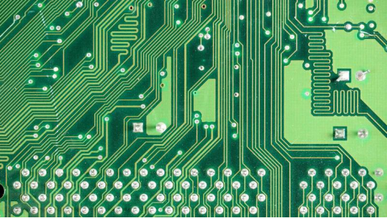
Do you know the deal with square traces on PCBs?

As you know, there are some certain rules you need to know as designing a PCB. For example, you should place decoupling capacitors near the power pins to each chip, it should be one gigantic fill of copper for your ground planes, and an antenna, which is made up of two ground planes that connected by a single trace. As well as analog sections should be held separate from digital sections, and it needs to isolate the section if you are dealing with high voltage.
We often hear that you can not place a 90 degree angle on a trace. However, some people are afraid that make it easy to have a situation, which is everyone will learn that you don’t know what you are doing if there is the mere sight of a 90 degree angle on a board. But does not it have any greater sin than a 90 degree trace on a PCB?
Needless to say, we have a better understanding of PCB design as the traditional wisdom of avoiding 90 degree traces. And you will unsatisfied as you find a PCB with 90 degree traces. How important is the square traces? The short answer is no, however, there is still a reason we don’t do it.
The effect of RF and capacitance
One of the reasons why 90 degree traces on a PCB is bad is that RF interference. But electrons bunch up on the corners is the most frequently used reason why you shouldn’t use square corners on traces. As far as our current understanding of physics is concerned, it is impossible and destroys the universe. But luckily, you can rent test equipment to test a circuit at 20 Gigahertz. What’s more, you will find the test equipment in the trash if you are really luck. This year, a electronic engineer put square corners to test by measuring the impedance of a trace that looks like a square wave. It is obvious that square corners will have a minimal effect at 20 Gigahertz, and it will have a less effect at lower frequencies. So don’t be afraid of square corners on your traces.
As you know, there will have a few effect on using 90 degree traces concerning RF interference, however, we have trouble with resistance of a trace because of the nature of square corners on traces. The resistance is a function of the trace shape, which is called a thin layer resistance. What’s more, the resistance of a trace is measured in Ohms per square. There are not any other dimensions for Ohms per square, it’s counter-intuitive when a square of copper two millimeters on a side has the same resistance as a square of copper ten millimeters on a side.
However, a 90 degree corner has a little effect on the resistance of a trace if it substitutes with a 45 degree corner, which is how does triangle work. Although there has a minor effect, it does make a difference in the capacitance of a trace. So something you need to pay attention, square corners do effect capacitance, however, it is not a real matter only if it has a short time for the circuit rise. As a official rule of thumb shows, when the line width in mils is greater than five times the rise time in picoseconds, a square corner will make an effect on the circuit. Only if you deal with relatively high-speed signals-the black magic of RF or SPI busses on the order of 100 MHz, it doesn’t matter.

Acid traps during PCB etching
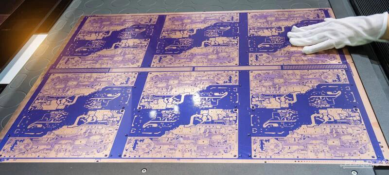
Acid trap is necessary to take into consideration in PCB fabrication. Many PCBs are working as a sheet of fiberglass or other substrate covered with a layer of copper, which is the raw material for each PCB manufacturer. It is different in the substrate, but the amount of copper on a PCB, everything starts with copper bonded to some sort of non-conductive material no matter what intermediary processes go into fabricating a board. You can mask off and remove the copper for turning the raw material into a PCB, which can be done with laser printer toner or Ultraviolet-cured photomask, then etch the copper with a chemical ( Ferric chloride, Sodium persulfate, or Cupric chloride). there are a lot of different methods to fabricate a PCB, but it is quite similar.
It’s possible for a “puddle”of the acid solution to gather at the corner of a trace as etching a PCB. If this happens, the acid is possible to corrode at copper underneath the photoresist. On the contrary, it will reduce the effective width of a trace so that completely breaking the trace. However, the skill to avoid acid traps has been for several decades, and it has improved greatly in PCB fabrication. So if you get trouble with acid etching copper in a corner, you should find a good PCB manufacturer.
If you have any questions, please feel free to contact us with service@pcbgogo.com, we will be happy to help you.


