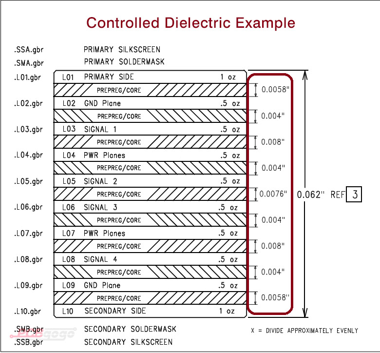
How to distinguish between controlled dielectric and controlled impedance?
There is some confusion about what is the difference between controlled dielectric and controlled impedance, and what are they? Now PCBGOGO will make an explanation for you.
How to distinguish between controlled dielectric and controlled impedance in PCB fabrication? Basically, what the purpose of controlling dielectric is the same as controlling impedance, achieving a goal of impedance on one or more signal lines of a PCB. For instance, your design has a USB signal pair, but it needs to have an impedance of 90 ohms ( ±10%) if you want to make it work properly. So there are a lot of factors requiring to be taken into consideration and calculated for ensuring it will happen, such as trace width, distance between copper features on other layers, spacing between copper features on the same layer, PCB manufacturing with the Dk ( dielectric constant ) of the laminate, as well as a few other factors.
Controlled dielectric

If you are an adventurous electrical engineer and you would like to solve the problem by yourself, you can control your own impedance with the controlled dielectric. And you need to know what kinds of dielectric spacing do you want between your copper layers in your fabrication as well as how to use your traces with the correct trace and space. So follow your design to meet the demands of impedance is what we need to do from a PCB manufacturing standpoint.
Controlled impedance
Controlled impedance is the characteristic impedance of a transmission line that is made up of PCB conductors. It’s related as high frequency signals are transmitting on the PCB transmission lines. And controlled impedance is important for signal integrity: it’s the propagation of signals without distortion.
The PCB impedance is determined by the physical dimensions and PCB materials. It’s measured in Ohms (Ω).

Some topics your need to know
Dielectric - the measure of resistance to the flow of electrical current, which is often known as Dk ( dielectric constant ).
On the other hand, dielectric means an electrical insulator that can be polarized by an applied electrical filed. Electric charges don’t flow through the material like in a conductor as a dielectric is placed in an electrical filed, but it is slightly shift from the average balance positions, which lead to dielectric polarization. Positive charges will move toward the field and negative charges shift in the opposite direction due to dielectric polarization. So it comes about an internal electric filed, which reduces the overall filed within the dielectric itself.
Controlled impedance - the match of substrate material properties with trace dimensions and locations, which create a specific electrical impedance for a signal moving alone a trace. Controlled impedance means that PCB manufacturing makes the impedance of traces within a certain percentage of a specified value.
Time Domain Reflectometry ( TDR ) - a measure of the reflections and spurious signals in a conductor resulting from the source coupling into non-ideal impedance ( such as the connecting wiring and termination ), which is a common test that used for high-speed digital and analog work.
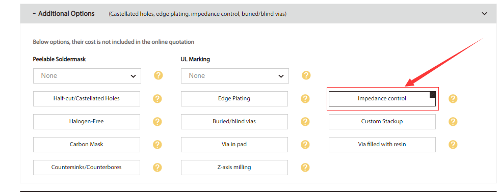
When you order your PCB with impedance control in PCBGOGO, we control the impedance by the dielectric thickness, the trace width and space. We run a TDR test to make sure the correct impedance is met. And we will try our best to meet the demands of customer and PCB manufacturing within the specified tolerance. Select impedance control on the PCB Instant Quote.

Please feel free to contact us with service@pcbgogo.com if you have any questions.
