Ultraviolet Lasers In PCB Manufacturing
As you know, the trend in PCB design toward smaller features at high densities is important to support the fast-growing market for high-teach consumer products, on the contrary, there is a great demand on ultraviolet (UV) lasers systems to meet the demands of new laser processing capabilities. Needless to say, ultraviolet lasers are one of the most versatile and efficient printed circuit board (PCB) processing technologies available. However, anyone working with PCB applications will be mistaken to overlook it. Now PCBGOGO will give a brief introduction for you.
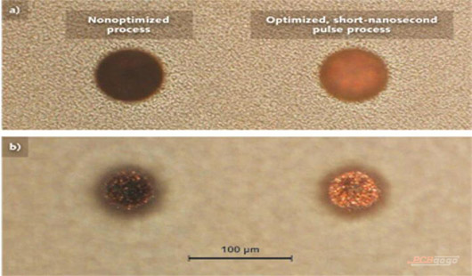
Introduction
PCB design promotes the development of electrical performance to further the performance and miniaturization of various devices, especially for consumer electronics such as tablets, smart phones, as well as GPS devices. What’s more, the necessary number and density of connections that connect with the devices interface is greatly improved with increasing integrated circuit (IC) fabrication.
On the contrary, there is a great demand on smaller and denser PCB features, including the micro-vias with small diameter, high-density interconnect (HDI) patterns. In addition, it will reduce the dimensional gap to wafer-level processing for the packages from multichip module (MCM) to ball grid array (BGA) and chip-scale packaging (CSP).
Ultraviolet (UV) lasers will be widely used in PCB fabrication to meet the demands of materials processing of designs. And it absorbs and cleanly ablate the energetic photons from UV lasers with a variety of materials, what’s more, the shorter wavelength allows tight focusing, which is good for fine-feature and high-intensity machining.
Surface etching
UV lasers does well in PCB fabrication, it etches surface patterns into boards in few minutes, which is the fastest method in PCB fabrication. R&D departments make a survey, there are more and more prototyping labs equipped with UV laser systems.
Ultraviolet laser beam can be in the range of 10-20μm based on optical calibration, and it needs to be seen that the manufacturing circuit trace with microscope to fabricate flexible circuit trace as it is infinitely small.
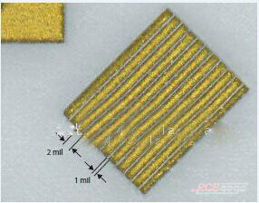
While fabricating the boards with a UV laser beam is the fastest method, the chemical technology is better to do surface etching in mass-scale because of the cost and product.
PCB depaneling
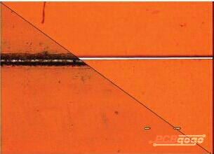
Ultraviolet laser cut is the optimal option for large or small manufacturing as well as PCB depaneling, especially for flexible or rigid-flex circuit board. Depaneling is getting rid of individual boards from a panel, but there is a great challenge with the increasing of flexible material. What’s more, there are some mechanical depaneling methods easy to damage sensitive and thin substrates, such as V-cut and routing, making trouble for electronic manufacturing.
Ultraviolet laser cut not only removes the effects of mechanical stress in depaneling process, such as burring, deformation and damaging circuit component, but also makes a small effect on thermal stress for the optical laser depaneling, such as CO2 cutting.
This reduction in stress means a lot in today's age of miniaturization. It could save space with the reducing of cutting cushion, which is the best for efficiency to maximum the flexible circuit board as component is closer to the edge of the circuit and more circuits can fit on each panel, maximizing efficiency and pushing the limits of what is possible with flex circuit processing.
Drilling
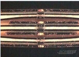
Drilling is the another application for lasers in PCB manufacturing. And it make use of UV laser’s small beam dimension and low stress properties, such as through hole, mircovias, blind and buried vias. What’s more, ultraviolet laser system is drilling with focused vertical beam to cut straight through the substrate, which is drilling with the hole of 10μm based on used material.
It’s useful for ultraviolet laser to do the multilayer drilling. Multilayer circuit board is to connect and hot press with composite material. And the attribute without press could be solve the problem for ultraviolet laser to make multilayer circuit board be “full curing” despite “semi curing” is detached. There is a key point: the data of yield is going up about ultraviolet laser’s low press attribute. And the rate of yield is the percentage of available and removed circuit boards on one panel.
There are a lot of cases leading to the broken of printed circuit board in manufacturing process, including bad solder joint, broken component or lamination. Which one would make printed circuit board cancel and invalidate in production line.
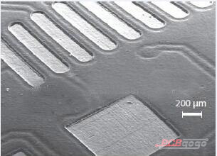
Engraving depth
Engraving depth is another application to display ultraviolet laser’s versatility, it including many types. And it could be cutting on some material based on required depth, stop, travel, as well as finish the manufacturing before turning to another depth and duty. There are various depth applications, such as pocket creation, useful for embedding chips, and skiving, the removal of organic material from metal.
Ultraviolet laser could operate with muti step on the substrate. First of all, come into being a flute of 2 mil depth with laser in polyethylene material, second, making a flute of 8 mil on the basic of last one, and then the flute with 10 mil. So it can be seen that ultraviolet laser system could be control the function with providing whole users.
Conclusion
In a word, the most striking of ultraviolet laser is that finishing all the above applications in a single step. So what’s the meaning for printed circuit board manufacturing? you don’t need to finish some application with effective process and way on different equipment, and it could be taking the complete component only one manufacture.
The streamline manufacturing method is good for removing the quality control problem for printed circuit board from one process to another process. And ultraviolet debris-free ablation qualities don’t need to do the post-processing cleaning. Needless to say, UV will be more than just a technology you shouldn’t overlook -- it will be something you can't miss.
