An Introduction of Organic Solderability Preservative (OSP) by PCBGOGO
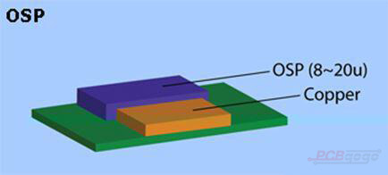
Over the years, electronic products are developing towards light, short, miniaturized and multi - functional. As well as high precision, high speed, high density and so on. However, hot air leveling process is increasingly unsuitable for the demands of PCB fabrication process as the rapid development of SMT. At the same time, the soldering material, such as Sn-Pb, which can’t meet the demands of environmental requirements for hot air leveling process. In a word, OSP is a chemical process with a layer of organic coating on the clean bare copper surface, which has heat shock, anti-oxidation and moisture resistance to prevent the copper surface from getting rusty ( oxidation or vulcanization ) in normal environment. But it needs to easily remove the protective film by the flux at subsequent soldering temperatures, so that the exposed clean copper surface can be connected with the molten solder in a minute to be a solid solder in a very short time.

Brief introduction
OSP is a process for surface treatment of PCB copper foil based on RoHS instructions, which get rusty in a normal environment with a water-based organic compound. But it needs to easily remove the protective film by the flux, so that the exposed clean copper surface can be connected with the molten solder spot in a very short time.

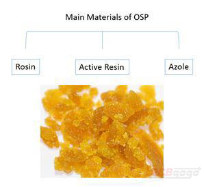
Main OSP materials:
1. Rosin
2. Azole
3. Active resin

OSP process flow:
There is the brief process for OSP as following:
Oil Removal→Second Level Washing→Micro Corrosion→Second Level Washing→Acid Washing→DI Washing→Film Formation→DI Washing→Dry
1. Oil removal:
The oil removal has a direct effect on the quality of film formation. And poor oil removal leads to uneven film thickness. On one hand, it can control the concentration beyond the scope of process by analyzing the solution. On the other hand, there will have a good effect as always checking the oil removal, however, it should change in time if the oil removal is bad.
2. Micro corrosion:
The aim of micro corrosion is to be a crude copper surface which is easy to do the film formation. And the thickness of micro corrosion has a direct effect on the film-forming rate. So it’s important to make the micro corrosion thickness be stable if being a stable film thickness. In general, the thickness of micro corrosion should be controlled at 1.0μm to 1.5μm that it’s more suitable, so it can make sure the micro corrosion time and rate based on the rate of micro corrosion before each production.
3. Film formation:
It will be better with DI washing both before and after the film formation. And the PH should be limited to between 4.0 and 7.0 to protect contamination of the film from being polluted. The key of OSP process is to control the thickness of anti-oxidation film, which make it easy to make an effect on soldering property. In general, the film thickness is suitable between 0.2μm to 0.5μm, for example, the thinner the film is, the poorer thermal shock capacity will be.
Disadvantages of OSP:
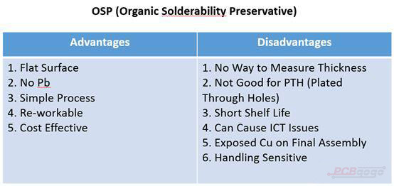
OSP certain has its disadvantages, for example all kinds of actual recipes and property. More importantly, it is extremely thin for the protective film and easy to scratch, so it needs to be carefully manipulated and transported. As well as OSP film will have an effect on solderability and reliability as it changes the color or crack. In other words, the certification and different industries in terms of quality, delivery, cost-effectiveness and any other demanding requests.

What could PCBGOGO do?
With over 10 years as an industry leader, PCBGOGO is one of the most experienced PCB and PCB assembly manufacturer in China. highly specialized not only in quick-turn PCB prototype and PCB assembly, but also medium and small volume PCB fabrication. And we will try our best to meet your PCB demands and committed to adhering to the strictest standards in PCB fabrication and assembly.
If you have any questions, please feel free to contact us with service@pcbgogo.com, we will be happy to help you.
