How to do a PCB assembly process work?
PCB assembly is a process that requires knowledge not just of PCB components and assembly but also of printed circuit board design, PCB fabrication and a strong understanding of the final product. Circuit board assembly is just one piece of the puzzle to delivering the perfect product the first time - without rework or assembly errors.
PCBGOGO’s printed circuit board assembly service is a leading turn-key solution for PCB fabrication and assembly under one roof specializing in small and medium volume PCB fabrication with fast lead-time and low minimum from 1pcs for PCBA. What’s more, we follow the reflow surface mount soldering requirements of the individual SMD components for each assembly job we do. We have a very high yield as we implement precise control of the reflow process.
PCB Assembly Process
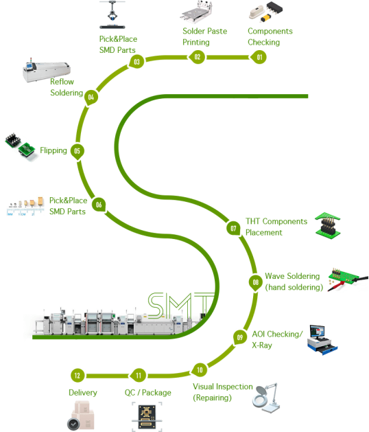
There are various stages necessary in the PCB assembly process, including adding solder paste to the circuit board, pick and place of SMD parts, soldering, AOI checking and inspection, test, which need to be monitored so as to fabricate the product with the highest quality.
Only very small volume PCB assemblies are handled manually and undergone by visual inspection, while the majority of larger projects are processed through reliable automated machinery. All soldering during the PCB assembly process is up to Class 1 standard, while Class 2 and Class 3 standard are also available for you to choose. PCBGOGO uses automated machinery to solder components on your PCBs with your pick & place CAD data at fast speed. Component positions, orientation and solder quality will normally be verified using Automatic Optical Inspection. AOI technology has proven to be extremely reliable whilst looking for errors in PCBs.
The PCB assembly process is below:
Solder Pasting
After component checking, you need to add solder paste to the circuit board. Solder paste is a paste of small grains of solder mixed with flux, and it’s used for reflow soldering of surface mount assemblies. Needless to say, solder paste plays an important role in PCB soldering, proving an easy to use medium for solder. Because of the advantages, it has been a simple and easy process, and it has a great effect on creating a connection between the leads or termination of surface mount components and pads/holes of PCB.
Pick and Place of SMD parts
Now pick and place of SMD parts have been completely automated in the PCB assembly process. The pick and place of SMD parts such as surface mount components, which were once done manually, are executed by robotic pick and place machines now. It can’t be denied that these machines can exactly place the components to the pre-planned areas of the circuit board.
Soldering
Once adding the SMD parts to the circuit board, the next stage of PCB assembly, the production process is to pass them through the soldering machine. Soldering technology plays an important role in the manufacturing of electronic products and their assemblies. And they have been widely used in electronic products because of soldering quality, performance, reliability, high accuracy and speed, and cost-effectiveness. There are two types of soldering for PCB assembly: wave soldering and reflow soldering. However, reflow soldering techniques are used more widely than using wave soldering.
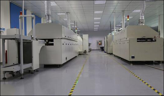
Reflow Soldering Process
It needs to place accurately the solder material on the board by using the soldering stencil. Then placing the components on the pads with a specialized pencil by the name “pick and place”. The reflow soldering process is as follows.
Preheating: preheating is compliance with thermal profile and does well in removing the volatile solvent that may include the solder paste.
Thermal soak: after the board is rising to the proper temperature, it will go into the thermal soak area. There are two reasons why the card is maintained at temperature, one is to make sure any areas that are not fully heated because shadowing effects come up to the necessary temperature. The other is to activate the flux and remove the solder paste solvents or volatiles.
Reflow soldering: the area of reflow is the area where it gets to the highest temperatures in the soldering process. The solder paste is melting here so as to create the necessary solder joints. And the practical reflow process involves the flux reducing the surface tension at the metal joint in order to achieve metallurgical bonding, allowing the individual solder powder spheres to melt and combine together.
Cooling: it needs to be done in a way without any stress to the components for the cooling boards after reflow. Appropriate cooling can restrain redundant intermetallic compound formation or thermal shock to the components. The range of typical temperatures in the cooling zone is 30-100℃ ( 86-212°F ), which is creating the relatively quick cooling rate. It can be a great grain structure in the solder with this method to offer the most mechanically sound joint.
AOI checking and Inspection
AOI checking: In PCBGOGO, AOI is one tool we use to provide the high-quality circuit boards for our customers. It works and identifies assembly errors with cameras and image processing software, such as soldering short circuits, missing or misplaced components, and disconnected components. As well as AOI improves the error detection over the visual inspection with more complicated PCBs and larger production quantity. AOI machine has been widely used in PCB manufacturing because the surface mount components have miniaturized and PCB production is mainly in making an effect.
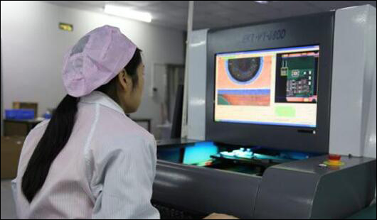
Inspection: automated X-RAY inspection is a technology based on the same principles as automated optical inspection. It uses X-rays as its source, instead of visible light, to automatically inspect features, which are typically hidden from view. Now X-ray inspection has been widely used in PCB assembly process in PCBGOGO. It’s able to find faults such as opens, shorts, insufficient solder, excessive solder, missing electrical parts, and mis-aligned components. Defects are detected and repaired within short debug time.
Test
It’s necessary to do the strictest test for your electronic products before shipping out. There are several methods in which they may be tested.
Packing and Shipping
After production and testing, your PCB orders will be packaged and sent to our shipping department. As the quick turn PCB manufacturer, PCBGOGO shipping department will ship your PCB quickly without any pending. For example, the 24 hours express PCB order will be shipped out in 24 hours after it is fabricated. The same follows for the 48 hours express.
PCB Assembly Quote and Order
Please combine the following files into a single ZIP file and contact us for a quick and non obligatory quotation.
1. PCB files
PCB file should be provided when you need PCB assembly services. PCBGOGO accepts Gerber file(RS-274-X), .PCBDOC, .PCB, Eagle file and etc. These listed files are required for PCB fabrication, testing and SMT stencil production; and will also be used to test the boards after soldering is completed.
2. Pick and Place (Centroid)
It is essential to send us the pick & place machine component placement data. This data will be used in PCBA production process by automatic PCBA machine. There will be columns for:
★ Surface Legend (top or bottom)
★ X/Y coordinate of the centre of the part (centroid data)
★ Part number
★ Rotation (theta)
★ In order to assemble your PCB smoothly, you could offer us some documents like 3D design file, schematics etc. to guide our PCBA process.
3. Bill of Materials (BOM)
Information provided must be in machine readable format (Excel or CVS). Your BOM should include:
Quantity of each part
Reference designator
Vendor and/or MFG Part Number (Digi-Key, Mouser, etc.)
Part description
Package description (QFN32, SOIC, 0805, etc. package is very helpful but not required).
Type (SMT, Thru-Hole, Fine-pitch, BGA, etc.).
Review Your Order & Send us Your Parts
Once you've reviewed your quotation and decided to order, it’s now time so send us your parts (we will provide an order number to include in your shipment). Notes:
1. Ship your package(s) using the pre-printed shipping labels your account manager will provide.
2. If there are parts from more than one order in the package be sure to segregate and clearly label them with the appropriate order numbers. If parts or boards are being drop-shipped from another company, make sure they put your order number on the packing slip.
3. Keep parts in moisture proof and/or anti static packaging.
4. Clearly label all parts and confirm that the labels match what you put in the BOM that you emailed to us.
5. Once we received your shipment we will confirm all order details.
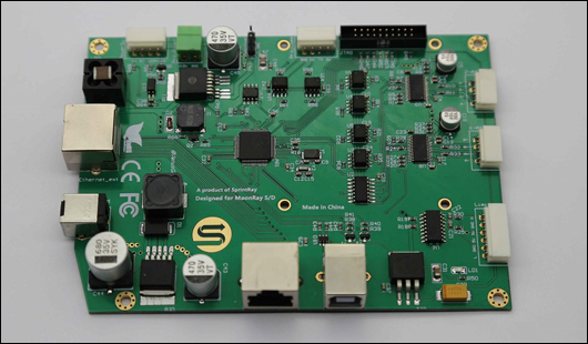
Quick Turn turn-key PCB Assembly in PCBGOGO
We can offer you a complete turn-key PCB assembly, working with you from the design phase through to product completion, saving you time and hassles.
PCBGOGO has a series of fully independent surface mount assembly lines with automatic machines like YAMAHA assembly machines, providing a theoretical capability in excess of 20,000 placements per hour. The lead time of PCB assembly prototype will be offered as rapidly as 24 hours. Mass production is supplied with a rapid assembly process within 3-4 days as well. We offer the most efficient SMT and through hole PCB assembly to process your order in time. Most of our work is scheduled; re-orders indicate that the customers believe we are reliable, competent and cost-effective.
