What Is Automated Optical Inspection (AOI) in A PCB?
When it comes to PCB fabrication, automated optical inspection (AOI) is an important process used in PCB fabrication and PCB assembly, as well as a test for printed circuit boards. It plays an effective and accurate role in detecting the electronic assemblies and your PCBs to make sure the product has a high quality leaving the production line and your PCB without any manufacturing faults.
What is Automated Optical Inspection (AOI)?
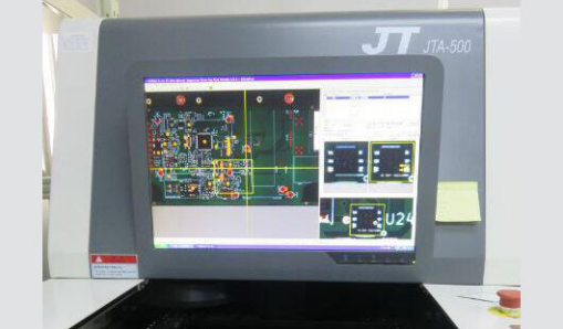
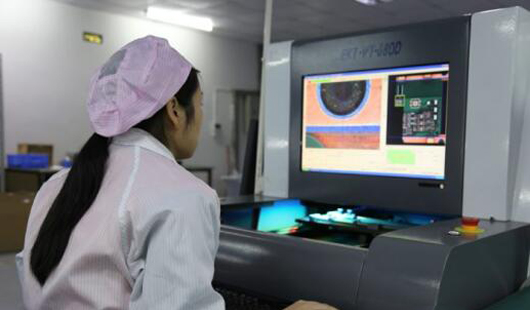
Automated optical inspection (AOI) is a machine-based technique used to test and check PCB for potential errors, such as surface defects, dimensional defects, as well as component placement defects. As the circuit board is more and more complicated, it’s hard and impossible to manually check the boards, needless to say, AOI plays an important role in checking the printed circuit board after assembly. What’s more, it does make a great effect on getting the necessary product quality in the production line with low cost.

In PCBGOGO, AOI is one tool we use to provide the circuit boards with high quality for our customers. It does work and identify assembly errors with cameras and image processing software, such as soldering short circuits, missing or misplaced components, and disconnected components. As well as AOI improves the error detection over visual inspection with more complicated PCBs and larger production quantity. AOI machine has been widely used in PCB manufacturing because the surface mount components have miniaturized and PCB production is mainly in making an effect.
The advantages of automated optical inspection
Positional accuracy: With the size of components decrease, the positional accuracy of both inspection equipment and manufacturing are increasingly important. And AOI system should have sub-pixel accuracy as a rule-of-thumb, which make sure the there is enough accurate for the system to detect the small deviations in position that can result in a 01005 defect.
Low cost: AOI test can improve the pass rate of PCB so that reduce the PCB cost.
Multiple inspection objects: AOI test not only works well used in PCBs, but also for PCB assembly. As to PCB, it checks the defects, for example, shorts, opens and insufficient solder. However, for PCB assembly, it inspects some questions, such as component soldering, polarity and values.
Programmable lighting: It’s important for lighting to achieve the desired results in any machine vision application. Considering the constantly changing environment of electronics fabrication, it’s impossible to find one light source that can detect all defect conditions. So a dynamic light is so important to make sure the component and PCB configurations have the widest defect coverage. As the cost reduction of light-emitting diodes, AOI test can configure light arrays that are highly customizable within the inspection software. What’s more, AOI test can flexibly increase the contract of image so that make it easy to identify a multitude of defect conditions with multiple colors at different angles. Programming lighting is an invaluable tool to make sure the widest range of detect detection.
Network capable software: One important function of any AOI system is data collection and retrieval. The data can be in the form of a text output, image collection, database, or a combination of several formats. Collecting the data is a basic function of most AOI systems, but, retrieving the information is often more complex and depends on the configuration of the manufacturing line.
Good Flexibility: AOI can be used in any stage of fabrication process based on the needs and cost tolerance capacity. And the reason why it’s better to do AOI test after reflow soldering is that most of defects are the result of failure in the soldering process so that reduce corresponding cost and increase inspection efficiency. As well as it can modify immediately the fabrication or assembly parameters to manufacture correctly the subsequent products.

So why is AOI so important?
If your PCB design is correct, and you assemble the right components in the right place, then your product will work. In production, it will focus on detecting and correcting any fabrication defects or manufacturing defects analysis. There is no doubt that AOI is important inspection system to test and check the quality of your PCB fabrication, as well as correct any problems or defects at any strategic point in the process flow. The most important thing is that AOI is the quality gate for your printed circuit board, which make sure that we can provide your board with a high quality for you.
In many ways, your PCB board plays an important role in electronic products and is the brains of your product, so it’s a vital component with its own accurate and rigid design demands. What’s more, printed circuit board will be more and more complicated just like PCB is getting smaller. Even though a quite simple board that can be made up of thousands of soldered joints, which means manual check may be workable or not.
So the sooner finding the faults in the manufacturing process, the easier the more cost-effective to avoid replicating the same problem on a larger scale.
In a word, AOI is necessary for you if you’re in the business of creating PCBs.
What kinds of defects can be checked during AOI?
AOI can check the surface defects (such as nodules and scratches), and dimension defects (for example open circuits, short circuits and thinner solder), as well as wrong components, missing components, and wrong placed components.
For a PCB with components (SMT inspection): insufficient solder joints, height defects, wrong part, solder bridging, excessive solder joints, billboarding, volume defects, tombstoning, component offset, component polarity, component presence or absence, component skew, area defects, flipped component, insufficient paste around leads, lifted leads, no population tests, paste registration, and severely damaged compoments.
For PCB board: short circuits, line width violations, spacing violation, excess copper, missing pad, cuts, incorrect mounting of components, as well as hole breakage (whether via is going outside of its pad).
AOI application areas
Short circuits
Line width violations
Spacing violations
High frequency
Excess copper
Missing pad
High power loads

Conclusion
In a word, it can check the quality of the boards coming off the end of the line for any PCB fabrication area. Only in this way can they monitor quality and rectify the process as detecting there have the problems so that it won’t make an effect on other boards. In this way, automatic optical inspection and X-Ray inspection are necessary tools for the PCB fabrication industry. And we will be committed to adhering to the strictest standards in manufacture and assembly with AOI and X-Ray inspection.
