What Is Copper Based PCB?
1. What is copper based PCB?
2. The types of copper based PCB
3. The advantages of copper based PCB
4. Thermoelectric separation copper based PCB
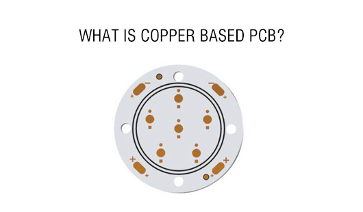
When it comes to metal core PCB, there are three types of materials in metal core PCB, such as aluminum PCB, copper based PCB, iron based PCB. However, as the high power electronic components have a great demand for PCB heat dissipation, the need for metal core PCB in the market is also increasing, what’s more, there is a higher processing demand for copper based PCB, which is widely used in the field where has a high power and high frequency PCB design. Because copper based PCB needs to have a great current carrying, it needs a thick copper foil, in general, the thickness of copper foil is 35μm~280μm. Copper based PCB can be etched the fine pattern and processed into a convex platform, the component can be connected to the platform so that it makes a great effect on grounding and heat dissipation.

What is copper based PCB?
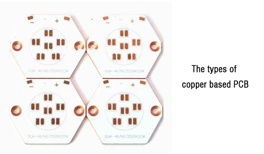
Copper based PCB is the most expensive in metal core PCB, which has a great thermal conductivity better than aluminum PCB and iron based PCB, applying to high frequency circuit design, and the areas where have a great change for high and low temperatures, as well as sophisticated communication equipment and architectural decoration industry. There are all kinds of copper based PCB, such as immersion gold copper based PCB, silver plating copper based PCB, hot air soldering leveling (HASL) copper based PCB, anti-oxidation copper based PCB and son on.
There is great demand for current carrying in copper based PCB layer so that creating a thicker copper foil with 35μm~280μm, thermal conductivity insulating layer makes a great effect on copper based PCB, and thermal conductivity is mainly made up of aluminum oxide and silicon powder, as well as the polymer filled with epoxy resin, what’s more, copper based PCB has a lot of advantages, such as low thermal resistance with 0.15, good viscoplastic property, ability to withstand thermal aging, as well as mechanical and thermal stress. Copper based PCB metal substrate plays an important role in copper based PCB, which is the support component of copper based PCB, mainly playing an important role in heat dissipation, shielding, covering or grounding. But it needs to have a high thermal conductivity, applying to some normal mechanical process, such as drilling, punching, and cutting and so on.
The types of copper based PCB
Immersion gold copper based PCB
Silver plating copper based PCB
Hot air soldering leveling (HASL) copper based PCB
Anti-oxidation copper based PCB

The advantages of copper based PCB
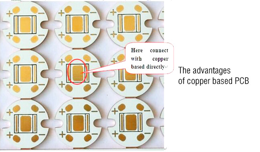
Comparing to aluminum PCB, copper based PCB has a great thermal conductivity which is the twice higher than aluminum PCB, the higher thermal conductivity is, the higher heat conduction is, as well as the better heat dissipation is. And copper base can be plated though hole but aluminum base can not, however, it needs to be the same for the network of plated through hole so that the signal has a great grounding property, still, the copper has the solderability to mount and solder the structural component of design in the end. What’s more, the copper base on the copper based PCB can etch a great drawing, there will a boss shape after processing, which is good for component, needless to say, the component can be directly pasted on the boss so that make a great effect on good grounding and heat dissipation. Because there is a different modulus of elasticity between copper and aluminum, such as for copper, its modulus of elasticity is about 121000MPa, but aluminum is about 72000MPa, and the warping and shrinking of copper based PCB is smaller than aluminum PCB, which has a more stable property.
● Low thermal resistance and high pressure resistance
● Excellent dimensional stability
● good heat dissipation
● Non-magnetic
● High mechanical strength
● Good viscoplastic property
● Ability to withstand thermal aging

The rules you need to know when you design the copper based PCB
The minimum drilling diameter needs to be 0.4mm because of thicker copper base, the thickness of copper foil on the copper based PCB determine how the line width and spacing are, if the copper foil is thicker, it will need more wider line width and larger minimum spacing.
Thermoelectric separation copper based PCB
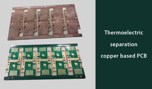
Thermoelectric separation based PCB: for the circuit layer, the circuit parts is not the same as the thermal layer part of the substrate, and the parts of thermal layer is directly in contact with the parts of lamp bead heat dissipation so that achieve the best heat dissipation and heat conduction (zero thermal resistance), which is generally called copper base.
The advantages of thermoelectric separation copper based PCB:
1. Apply to copper base, for based PCB, there is a high density and has a strong thermal load carrying ability and great heat conduction and heat dissipation.
2. Use the thermoelectric separation structure, and is in contact with zero thermal resistance to the lamp bead. So it can prevent the attenuation of lamp bead light from reducing and extend lamp life.
3. For copper base, it has a high density and great thermal load carrying ability, as well as smaller size at the same power.
4. Suitable for matching single high power lamp bead, especially COB package so that make a better effect.
5. It can do various surface finish based on different demands, such as immersion gold, OSP, hot air soldering leveling (HASL), silver plating, immersion silver + silver plating, there has a great reliability on the layer of surface finish.
6. It can make different structure according to different design needs of the lamps, such as copper bumps, copper concave block, the parallel thermal layers and circuit layers.
The disadvantages of thermoelectric separation copper based PCB:
It is not suitable for packaging with single electrode chip bare crystal.

PCBGOGO thermoelectric separation copper based PCB process steps:
1. First of all, cut the copper foil based PCB into a size that is suitable for processing.
2. Note that it needs to roughen the copper foil on the PCB surface with brushing, micro-etching and so on before squeezing film the based PCB.
3. Then, attach the dry film to the photoresist at an appropriate temperature and pressure, and it will create polymerization after being irradiated with ultraviolet light in the transparent area of the film, where the dry film will be reserved as an etching resist when developing and copper etching, however the circuit image on the film will be transferred to the dry film photoresist on the board.
4. Develop and remove the unexposed area on the film surface with an aqueous solution of sodium carbonate after peeling off the protective film on the film surface, and corrode and remove the exposed copper foil with a mixed solution of hydrochloric acid and hydrogen peroxide to form a circuit.
5. Finally, clean the dry film photoresist that has been finished with an an aqueous solution of sodium hydroxide. For six or more layers inner layer PCB, it can punch out the reference hole of the interlayer circuit with the automatic positioning punching machine.
