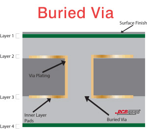
What is a "buried via" on an electronics PCB?
Buried Via is a copper plated hole that connects two or more internal layers of the board and is not accessible by the external layers. And it’s not possible to discover a buried vias in a PCB because it is "buried" under the external layer surfaces of the board. What’s more, buried vias also need an individual drill file.
A buried via in a PCB is fabricated with processing one or more double-sided PCBs. A very thin, double-sided core (2 layers within a multilayer PCB) is processed as a complete plated-through DSB, and it needs to have different process equipment from a standard double-sided PCB because of the thickness of the core-which can be as thin as a sheet of paper. However, it is necessary to have the through hole process expect the solder mask and final surface finish.

Benefits of buried vias
Prevent from signal interference;
Reduce the aspect ratio of the PCB;
Ability to meet the density constraints of line lines and pads on a typical design without increasing the layer count or PCB size;
Save the routing space;
Keep the continuity of transmission line about characteristic impedance;
Have not effect on the trace or surface mount component on the top or bottom layers of the board.
How to fabricate the PCB with buried vias?
As you know, buried vias need to remain invisible to the external layers. In other words, keep them buried. And you should make the traces that are necessary and stacks up to the internal layers as usual if you want to develop a buried via. After that, develop the vias and test them. In the end, you need to do the whole PCB package by stacking up to rhe external layers. So the package will have buried vias extruded in the middle.
Reduce your cost with buried vias in HDI PCB fabrication
Buried vias play an useful role in reducing the aspect ratio of the PCB. It usually needs an extra manufacturing cost as the aspect ratios is higher than 10 or 12 (note that the finished hole size is ~2mil less than the drilled hole size; this due to the width of the barrel plating). however, there can be reduce the PCB thickness and in turn the aspect ratio to reduce the overall manufacturing cost with buried vias.
In general, a PCB will have BGA components with several different pitches. Such as, there may be the BGA with 1.27mm pitch and 0.8mm pitch on a 4.0mm ( 160mil ) thick PCB. The minimum via hole is not only decided by drill hole, but also the aspect ratio, which is the ratio between the PCB thickness and diameter of the drilled hole, and the thickness of the PCB is divided by the diameter size of the drilled hole:

There may be a challenge to keep the aspect ratio low after using the buried vias if it needs the through hole vias. An aspect ratio of 12 on a 4mm PCB will mean that the size of the minimum finished through hole via is 0.3mm (12mil), which is corresponding to a drill hole size of 0.36mm(14mil) and pad size of 0.56mm(22mil). and it will have a great effect for the BGA with 1.27mm pitch, however, causing concerns for the BGA with 0.8mm pitch. Because the clearance from via pad to BGA pad is 0.09mm(3.4mil) with 0.4mm(15.7mil) BGA pads.
It need to reduce the PCB thickness as follows to meet the demands of aspect ratio:
3.6mm (140mil) for 10mil through-hole vias (drill size of 12mil) with 0.5mm (20mil) pads for the 0.8mm pitch BGA
3.0mm (120mil) for 8mil through-hole vias (drill size of 10mil) with 0.45mm (18mil) pad for the 0.8mm pitch BGA
It can achieve a smaller aspect ratio for your PCB and avoid any costs penalties because of buried vias if you reduce the layer count by replacing through-hole vias with buried vias.
HDI PCB fabrication with buried vias in PCBGOGO

PCBGOGO has specialized in PCB fabrication with buried vias with over 10 years. Both the engineers and production facility are equipped to deal with the intricacy this technique requirements, with high accuracy. It’s more costly for this technique, but we have been saving your cost with reducing the PCB layers or size, which is more and more popular in the PCB industry.
Furthermore, if you still need more help or want to ask something, we are always here for you. Simply contact us at service@pcbgogo.com or visit our website to get the best customer support. Our team of Engineers can easily handle the complexity the buried vias need and provide very high-quality work.
