What problems should we pay attention to when drawing PCB from soldering?
with the rapid development of electronic technology, it’s more and more prevalent for the electronic component’s miniaturization 、BGA、the chip with spacing of 0.3mm~0.5mm, and the electronic component has a higher demand on soldering process. Now it has a more sophisticated chip mounter to take place the manual solder, but there are many factors affecting the soldering quality. So PCBGOGO makes an introduction about what problems should we pay attention to when drawing PCB from soldering. It’s likely that leading to some problems, such as poor solder, pseudo soldering, and pad or PCB is broken as PCB repairs If you don’t pay.
一、The factors affecting PCB soldering quality
It need to be strictly controlled for PCB designer and soldering process、the level of soldering worker and so on from PCB layout to a PCB with high quality that is finished by all components. There are some factors affecting PCB soldering quality as the following: a drawing of PCB, the quality of PCB, the quality of component, the oxidation of component pin, solder paste’s quality, printing quality of solder paste, the accurate degree of chip mounter programming, assembly quality, temperature profile’s setting of reflow oven and so on.

Soldering works can’t do that is the process of PCB drawing. Because a person who designs the circuit doesn’t solder PCB and lack of soldering experience, they don’t know what affect the soldering; however, the workers in the soldering works, just take responsibility for fabrication and they don’t pat attention to analyse why is poor soldering, what’s more, lacking the experience of drawing PCB. There is no doubt that it’s difficult to make a connection.
-
Some advises when drawing PCB
There are some advises on drawing PCB for layout designer, we hope that you can avoid the poor drawing that affect the quality of soldering in the drawing process.
-
Tooling hole
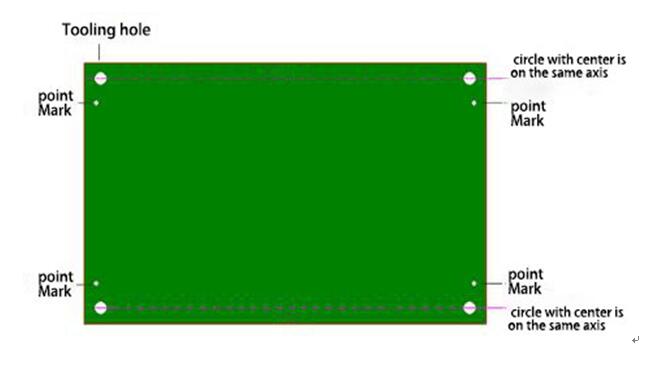
There should be four holes in the four corners of PCB( the minimum aperture is 2.5mm), which is used for positioning PCB as printing solder paste. The center of X or Y axis need to be on the same axis as the following drawing:

-
Point Mark
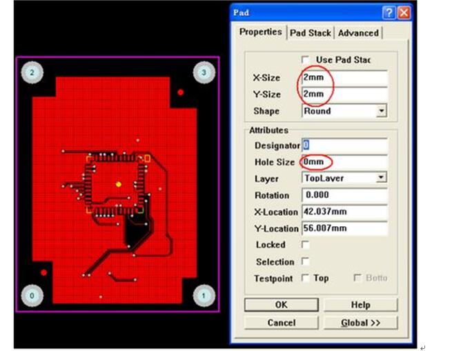
it’s used for chip mounter to position. Don’t forget to note the point Mark in the diagonal of board, it can be round or the pad of squareness, and don’t mix with other pad. It need to mark in both sides if the double side has components.
So please pay attention to the following points as do PCB layout:
a: the shape of point Mark as the following pattern.( the point Mark matches up in the center)
b. the dimension of A is 2.0mm.
c. There can’t be a change in shape and color that lead to false recognition within 2.0mm from the edge of point Mark. ( pad and solder paste)
d. copper plating or tin is preventing the surface from reflecting on the surface of point Mark to identify accuracy. Only the line is marked for shape, but the spot can’t identify.
As shown in the figure:

-
Leave the side about 5mm
There should be leaving the side with more than 3mm in the long direction to transfer PCB for chip mounter as drawing PCB, but it can’t be mounted devices within 5mm. So don’t place the mount devices within 5mm. As shown in the figure:
So we suggest that there is not mount devices within 5mm in the long direction of bottom side. And you can add break-up tab if it’s limited for the side of PCB.
-
No immediate via on the pad
The defect as you do the via immediately on the pad is that component pad is lack of tin to be pseudo soldering as solder paste flow into the via after melting when reflow. As shown in the figure:
-
Polarity label of diode and tantalum capacitors
It should conform to the rule to prevent the workers from soldering wrong by virtue of experience. As the figure:
-
Silkscreen and logo
Please hide the component model,especially a PCB with high density. Otherwise, it will affect finding the position of soldering as the complex. As the following figure:
Don’t forget to mark the tag when do the label. It can be seen that the chip mounter can’t work when programming as the following figure.
The font size of silkscreen can’t be too small to see clearly. It need to stagger the via for silkscreen placing to prevent misunderstanding.
-
Extend IC pad
It should extend the pad as drawing PCB for IC package, such as SOP、PLCC、QFP, it’s more suitable for the pad =IC pin ×1.5 on PCB so that the chip pin, pad and tin are melting together when manual soldering with solder iron. It can be seen as the following figure:
-
The width of IC pad
It should pay attention to the width of pad when drawing PCB for IC package, such as SOP、PLCC、QFP,the width of pad a is the width of IC pin on PCB( the value of Nom.in the datasheet), so don’t broden to make sure that it has enough width for b( two pads) to prevent soldering continuously. As the following figure:
-
Don’t rotate random angle as placing the devices
It’s only for 90℃、180℃、270℃、360℃ because mounter can’t rotate random angle. It rotates 1℃ as the following figureB, which make an effect on the quality of solder as the angle of 1℃ is staggered between the pad of devises pin and PCB after mounting.
-
The problem to be paied attention to when short circuit for contiguous pin
The short circuit way is bad for identifying the pin whether is bonding or not, and it’s not good after soldering.However, there will be a different soldering if short and add solder mask based on the ways of figure b and c when drawing. Only to divide the pins can’t the chip short, and have a good looking.
-
A pad problem under the chip
There is a pad under the chip it’s easy to lead to the problem of short if drawing the centre pad based on the package of chip as drawing. So it should be shorten the pad in the middle to increase the distance between and pin so that avoid the probability of short. As the following figure:
-
Two divices with high thickness should be arranged properly
It can be seen that it will impact the finished devices as mount the second devices, and tthere will lead to the problem of automatic power off due to it wil test the danger.
13、BGA
It can’t be seen that there is a soldering effect outise as the pads are under the chip because BGA package is particular. So we suggest that punching two tooling holes with 30mil to position the stencil as repair.
Tips: the tooling hole is not suitable for oversize or undersize, don’t drop and shake the needle after inserting, and it’s suitable to have a slightly tight insertion to avoid the suitation of uncorrect tooling. As the following figure:
What’s more, there should be some places for devices around BGA so that it’s for the stencil scrape solder paste when repair.
14、The color of PCB
We suggest that there is no red PCB.It can’t be programming and make it inconvenient to solder for mounter because the red PCB is white under the red light of mounter camera.
15、The small devices under the big
Someone like to put the small devices under the same layer of big devices, such as, there is resistance under nixie tube as the following figure:
It’s difficult to repair based on such setting and even lead to the damage of nixie tube, so don’t forget to dismantle the nixie tube as repair. As it can be seen in the figure:
-
Tin melting is affected by copper clad and pad
It can’t make full melt for tin solder to be pseudo soldering as the copper clad will absorb mass heat, as the following figure:
The pad is directly bondig with copper clad in figure a; the connector of 50Pins is not directly bonding with copper clad, but there are copper clad in large area in the middle two layers of four-layer board, so it can’t make full melt for solder paste as copper clad is absorbed mass heats in figure a and b. the body of connector 50Pins is a material of heat resistance, it will be melting or bending if there is a high temperature, otherwise the solder paste can’t make full melt as copper clad absorbs mass heats. So we suggest that the pad is isolated with the copper clad in large area. It can be seen in the figure:
17、The suggestion of panel and break away tab:
三、Conclusion
Now more and more designers are routing and designing PCB as drawing with software, but it can improve greatly the efficiency of soldering once finishing layout, so every designer should take it considerable to greatly communicate with PCB manufacturer and have the habit of drawing well.
